Multiple JK-BMS Modbus RJ485 integration
Principle of operation
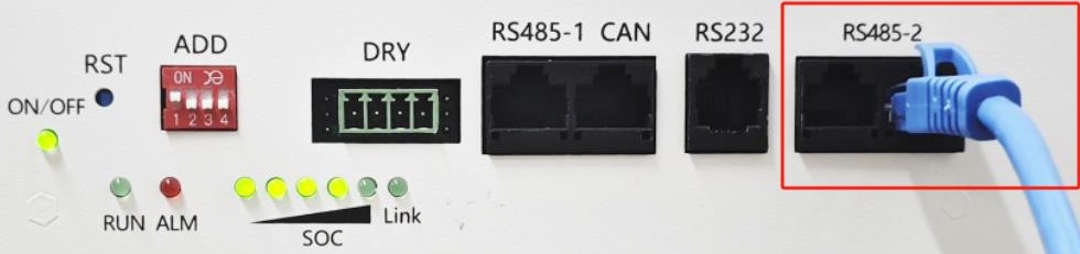
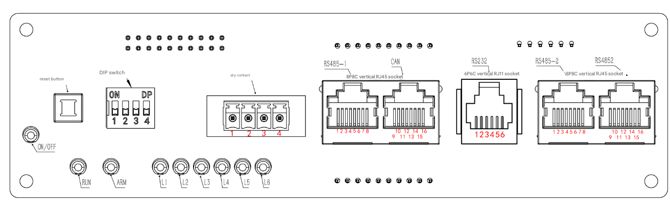
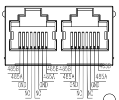
Communication Module Ports
Connections and wiring
Communication board
Configuration of the Communication Board presented below is verified and validated.
( Warning: Some available documents and manuals contain incorrect description of ports)
 |
|---|
 |
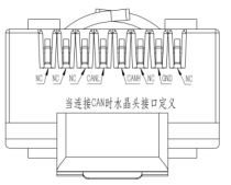
| Port 1 (UART1) RJ485 cable: | CAN Port cable: |
|---|---|
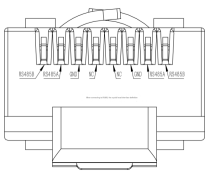 |
 |
| Port 2 (UART2) wiring: |
|---|
 |
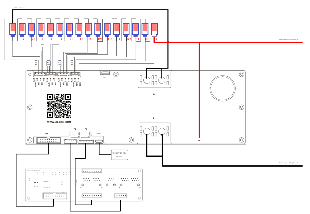
JK-BMS board
| JK-BMS board connectors: |
|---|
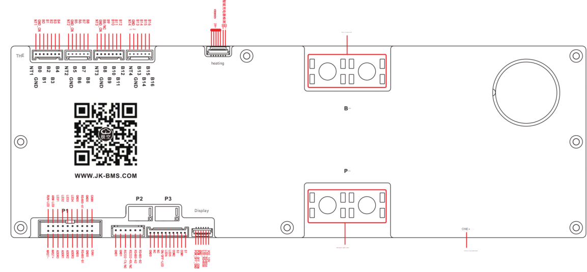 |
| JK-BMS wiring: |
|---|
 |
UART2 configuration
In the last software version only two protocols are available:
- 001 - JK BMS RS485 Modbus V1.0
- 015 - UART Protocol 015
Protocols are set not selectable by BLE configuration or Modbus.
UART1 configuration
The following protocols are supported on the RJ485-1 (UART1) port:
(italic options ane not settable)
- 000 - 4G-GPS Remote module Common protocol V4.2
- 001 - JK BMS RS485 Modbus V1.0
- 002 - NIU U SERIES
- 003 - China tower shared battery cabinet V1.1
- 004 - PACE_RS485_Modbus_V1.3
- 005 - PYLON_low_voltage_Protocol_RS485_V3.5
- 006 - Growatt_BMS_RS485_Protocol_1xSxxP_ESS_Rev2.01
- 007 - Voltronic_Inverter_and_BMS_485_communication_protocol_20200...
- 008 - China tower shared battery cabinet V2.0
- 009 - WOW_RS485_Modbus_V1.3
- 010 - JK BMS LCD Protocol V2.0
- 011 - UART1 User customization
- 012 - UART2 User customization
- 013 - (9600)JK BMS RS485 Modbus V1.0
- 014 - (9600)PYLON_low_voltage_Protocol_RS485_V3.5
- 015 - UART Protocol 015
CAN port configuration
The following CAN protocols are supported on the CAN port:
(italic options ane not settable)
- 000 - JK BMS CAN Protocol (250K) V2.0
- 001 - Deye Low-voltage hybrid inverter CAN communication protocol V1.0
- 002 - PYLON-Low-voltage-V1.2
- 003 - Growatt BMS CAN-Bus-protocol-low-voltage_Rev_05
- 004 - Victron_CANbus_BMS_protocol_20170717
- 005 - MEGAREVO_Hybird_BMSCAN_Protocol_V1.0
- 006 - JK BMS CAN Protocol (500K) V2.0
- 007 - INVT BMS CAN Bus protocol V1.02
- 008 - GoodWe LV BMS Protocol (EX/EM/S-BP/BP)
- 009 - FSS-ConnectingBat-Tl-en-10 | Version 1.0
- 010 - MUST PV1800F-CAN communication Protocol1.04.04
- 011 - LuxpowerTek Battery CAN protocol V01
- 012 - CAN BUS User customization
- 013 - CAN BUS Protocol 013
- 014 - CAN BUS Protocol 014
Communication protocol
UART2 usage
If Device Address is set to 0x00 (by the switches) then UART2 protocol is set to 015 and the master mode of the JK BMS RS485 Modbus V1.0 protocol is set.
During every 15 sec. status of the master device is send to the bus, followed by data request addressed to the all 15 slaves:
master    >>> 55 AA EB 90 02 00 C7 0C C7 0C C7 0C C7 0C C7 0C C7 0C C7 0C C7 0C C7 0C C7 0C C8 0C C7 0C C8 0C C7 0C C8 0C C8 0C 00 00 00 00 00 00 00 00 00 00 00 00 00 00 00 00 00 00 00 00 00 00 00 00 00 00 00 00 00 00 00 00 FF FF 00 00 C7 0C 01 00 00 01 3E 00 3B 00 3D 00 3B 00 3E 00 3B 00 3D 00 3B 00 3E 00 3C 00 3E 00 3C 00 3E 00 3D 00 3F 00 3D 00 00 00 00 00 00 00 00 00 00 00 00 00 00 00 00 00 00 00 00 00 00 00 00 00 00 00 00 00 00 00 00 00 BD 00 00 00 00 00 70 CC 00 00 00 00 00 00 00 00 00 00 A9 00 AD 00 00 00 08 00 00 00 00 41 6B 18 03 00 90 CA 04 00 00 00 00 00 FB 01 00 00 64 00 00 00 D8 FF 03 00 01 01 00 00 00 00 00 00 00 00 00 00 00 00 00 00 FF 00 01 00 00 00 AF 03 00 00 00 00 5E 48 3F 40 00 00 00 00 71 14 00 00 00 01 01 01 00 06 00 00 72 70 26 00 00 00 00 00 BD 00 AE 00 A8 00 AB 03 7F B8 1F 09 05 00 00 00 80 51 01 00 00 00 02 03 A5 67 00 00 00 00 00 00 00 FE FF 7F DC 2F 01 01 B0 0F 00 00 00 C5
master    >>> 00 10 16 20 00 01 05 9A
master    >>> 55 AA EB 90 01 00 AC 0D 00 00 14 0A 00 00 3C 0A 00 00 42 0E 00 00 FC 0D 00 00 0A 00 00 00 06 0E 00 00 28 0A 00 00 10 0E 00 00 AC 0D 00 00 C4 09 00 00 40 9C 00 00 03 00 00 00 3C 00 00 00 F0 49 02 00 2C 01 00 00 3C 00 00 00 05 00 00 00 E8 03 00 00 BC 02 00 00 58 02 00 00 BC 02 00 00 58 02 00 00 14 00 00 00 46 00 00 00 20 03 00 00 BC 02 00 00 10 00 00 00 01 00 00 00 01 00 00 00 01 00 00 00 90 CA 04 00 DC 05 00 00 B8 0B 00 00 00 00 00 00 00 00 00 00 00 00 00 00 00 00 00 00 00 00 00 00 00 00 00 00 00 00 00 00 00 00 00 00 00 00 00 00 00 00 00 00 00 00 00 00 00 00 00 00 00 00 00 00 00 00 00 00 00 00 00 00 00 00 00 00 00 00 00 00 00 00 00 00 00 00 00 00 00 00 00 00 00 00 00 00 00 00 00 00 00 00 00 00 00 00 00 00 00 00 00 00 00 00 00 00 00 00 00 00 00 00 00 00 00 00 00 00 00 00 00 00 00 00 00 00 00 00 00 00 00 00 00 00 00 00 00 00 60 E3 16 00 00 32 3C 32 18 FE FF FF FF 9F E9 1D 02 00 00 00 00 C7
master    >>> 00 10 16 1E 00 01 64 56
master    >>> 01 10 16 20 00 01 02 00 00 D6 F1
slave  01 <<< 55 AA EB 90 02 05 C4 0C C4 0C C4 0C C4 0C C4 0C C4 0C C4 0C C3 0C C4 0C C4 0C C4 0C C4 0C C4 0C C4 0C C4 0C C4 0C 00 00 00 00 00 00 00 00 00 00 00 00 00 00 00 00 00 00 00 00 00 00 00 00 00 00 00 00 00 00 00 00 FF FF 00 00 C4 0C 01 00 00 05 3A 00 37 00 3A 00 37 00 3A 00 38 00 3A 00 37 00 3B 00 39 00 3B 00 38 00 3B 00 3A 00 3C 00 3A 00 00 00 00 00 00 00 00 00 00 00 00 00 00 00 00 00 00 00 00 00 00 00 00 00 00 00 00 00 00 00 00 00 AE 00 00 00 00 00 3F CC 00 00 00 00 00 00 00 00 00 00 A7 00 AC 00 00 00 08 00 00 00 00 40 CA 14 03 00 90 CA 04 00 00 00 00 00 16 02 00 00 64 00 00 00 A8 FF 03 00 01 01 00 00 00 00 00 00 00 00 00 00 00 00 00 00 FF 00 01 00 00 00 A8 03 00 00 00 00 9C D7 3E 40 00 00 00 00 6C 14 00 00 00 01 01 01 00 06 00 00 F4 6B 26 00 00 00 00 00 AE 00 AB 00 A9 00 A4 03 80 B8 1F 09 03 00 00 00 80 51 01 00 00 00 01 00 49 6D 00 00 00 00 00 00 00 FE FF 7F DC 2F 01 01 B0 0F 00 00 00 2D
slave  01 <<< 01 10 16 20 00 01 04 4B
master    >>> 01 10 16 1E 00 01 02 00 00 D2 2F
slave  01 <<< 55 AA EB 90 01 05 AC 0D 00 00 14 0A 00 00 3C 0A 00 00 42 0E 00 00 FC 0D 00 00 0A 00 00 00 06 0E 00 00 28 0A 00 00 10 0E 00 00 AC 0D 00 00 C4 09 00 00 40 9C 00 00 03 00 00 00 3C 00 00 00 F0 49 02 00 2C 01 00 00 3C 00 00 00 05 00 00 00 E8 03 00 00 BC 02 00 00 58 02 00 00 BC 02 00 00 58 02 00 00 14 00 00 00 32 00 00 00 E8 03 00 00 20 03 00 00 10 00 00 00 01 00 00 00 01 00 00 00 01 00 00 00 90 CA 04 00 DC 05 00 00 B8 0B 00 00 00 00 00 00 00 00 00 00 00 00 00 00 00 00 00 00 00 00 00 00 00 00 00 00 00 00 00 00 00 00 00 00 00 00 00 00 00 00 00 00 00 00 00 00 00 00 00 00 00 00 00 00 00 00 00 00 00 00 00 00 00 00 00 00 00 00 00 00 00 00 00 00 00 00 00 00 00 00 00 00 00 00 00 00 00 00 00 00 00 00 00 00 00 00 00 00 00 00 00 00 00 00 00 00 00 00 00 00 00 00 00 00 00 00 00 00 00 00 00 00 00 00 00 00 00 00 00 00 01 00 00 00 00 00 00 00 60 E3 16 00 00 32 3C 32 18 FE FF FF FF 9F E9 1D 02 00 00 00 00 E6
slave  01 <<< 01 10 16 1E 00 01 65 87
master    >>> 02 10 16 20 00 01 02 00 00 C2 01
master    >>> 03 10 16 20 00 01 02 00 00 CF 91
master    >>> 04 10 16 20 00 01 02 00 00 E9 A1
master    >>> 05 10 16 20 00 01 02 00 00 E4 31
master    >>> 06 10 16 20 00 01 02 00 00 F0 C1
master    >>> 07 10 16 20 00 01 02 00 00 FD 51
master    >>> 08 10 16 20 00 01 02 00 00 BC A1
master    >>> 09 10 16 20 00 01 02 00 00 B1 31
master    >>> 0A 10 16 20 00 01 02 00 00 A5 C1
master    >>> 0B 10 16 20 00 01 02 00 00 A8 51
master    >>> 0C 10 16 20 00 01 02 00 00 8E 61
master    >>> 0D 10 16 20 00 01 02 00 00 83 F1
master    >>> 0E 10 16 20 00 01 02 00 00 97 01
master    >>> 0F 10 16 20 00 01 02 00 00 9A 91
more data can be foun in the /docs/log catalog of the JK-BMS project.
If Device Address is set to 1 - 15 (0x01 - 0x0F) then BMS is in the Modbus slave mode and protocol is set to 001
UART1 Usage
Port RJ485-1 is always ( required verification ) in the slave mode, even if Device Address is 0x00.
Our Hass integration is using JK BMS RS485 Modbus V1.0 (001) protocol.
More information: JK-BMS Modbus RS485 HASS ESPhome integration
Supported registers
Our integration supports all documented ports
Jikong BMS RS485 Modbus Universal Protocol V1.1 - Click to expand
Register Map
Start address code offset Index Data type Length R/W Data content Content Unit Note Note
Address
Field HEX DEC Type Length Unit
0x1000 0x0000 0 UINT32 4 RW Entering sleep voltage VolSmartSleep mV
0x0004 4 UINT32 4 RW Cell undervoltage protection VolCellUV mV
0x0008 8 UINT32 4 RW Cell undervoltage protection recovery VolCellUVPR mV
0x000C 12 UINT32 4 RW Cell overcharge protection VolCellOV mV
0x0010 16 UINT32 4 RW Cell overcharge protection recovery voltage VolCellOVPR mV
0x0014 20 UINT32 4 RW Trigger balanced voltage difference VolBalanTrig mV
0x0018 24 UINT32 4 RW SOC-100% voltage VolSOC100% mV
0x001C 28 UINT32 4 RW SOC-0% voltage VolSOC0% mV
0x0020 32 UINT32 4 RW Recommended charging voltage VolCellRCV mV
0x0024 36 UINT32 4 RW Float charge voltage VolCellRFV mV
0x0028 40 UINT32 4 RW Automatic shutdown voltage VolSysPwrOff mV
0x002C 44 UINT32 4 RW Continuous charging current CurBatCOC mA
0x0030 48 UINT32 4 RW Charge overcurrent protection delay TIMBatCOCPDly S
0x0034 52 UINT32 4 RW Charge overcurrent protection release TIMBatCOCPRDly S
0x0038 56 UINT32 4 RW Continuous discharge current CurBatDcOC mA
0x003C 60 UINT32 4 RW Discharge overcurrent protection delay TIMBatDcOCPDly S
0x0040 64 UINT32 4 RW Discharge overcurrent protection release TIMBatDcOCPRDly S
0x0044 68 UINT32 4 RW Short circuit protection release TIMBatSCPRDly S
0x0048 72 UINT32 4 RW Maximum balancing current CurBalanMax mA
0x004C 76 INT32 4 RW Charging over-temperature protection TMPBatCOT 0.1°C
0x0050 80 INT32 4 RW Charge over temperature recovery TMPBatCOTPR 0.1°C
0x0054 84 INT32 4 RW Discharge over temperature protection TMPBatDcOT 0.1°C
0x0058 88 INT32 4 RW Discharge over temperature recovery TMPBatDcOTPR 0.1°C
0x005C 92 INT32 4 RW Charging low temperature protection TMPBatCUT 0.1°C
0x0060 96 INT32 4 RW Charging low temperature recovery TMPBatCUTPR 0.1°C
0x0064 100 INT32 4 RW MOS over temperature protection TMPMosOT 0.1°C
0x0068 104 INT32 4 RW MOS over temperature protection recovery TMPMosOTPR 0.1°C
0x006C 108 UINT32 4 RW CellCount CellCount string
0x0070 112 UINT32 4 RW Charging switch BatChargeEN 1: open; 0: close
0x0074 116 UINT32 4 RW Discharge switch BatDisChargeEN 1: open; 0: close
0x0078 120 UINT32 4 RW Balance switch BalanEN 1: open; 0: close
0x007C 124 UINT32 4 RW Battery design capacity CapBatCell mAH
0x0080 128 UINT32 4 RW Short circuit protection delay SCPDelay us
0x0084 132 UINT32 4 RW Balanced start voltage VolStartBalan mV
0x0088 136 UINT32 4 RW Connection line internal resistance 0 CellConWireRes0 uΩ
0x008C 140 UINT32 4 RW Connection line internal resistance 1 CellConWireRes1 uΩ
0x0090 144 UINT32 4 RW Connection line internal resistance 2 CellConWireRes2 uΩ
0x0094 148 UINT32 4 RW Connection line internal resistance 3 CellConWireRes3 uΩ
0x0098 152 UINT32 4 RW Connection line internal resistance 4 CellConWireRes4 uΩ
0x009C 156 UINT32 4 RW Connection line internal resistance 5 CellConWireRes5 uΩ
0x00A0 160 UINT32 4 RW Connection line internal resistance 6 CellConWireRes6 uΩ
0x00A4 164 UINT32 4 RW Connection line internal resistance 7 CellConWireRes7 uΩ
0x00A8 168 UINT32 4 RW Connection line internal resistance 8 CellConWireRes8 uΩ
0x00AC 172 UINT32 4 RW Connection line internal resistance 9 CellConWireRes9 uΩ
0x00B0 176 UINT32 4 RW Connection line internal resistance 10 CellConWireRes10 uΩ
0x00B4 180 UINT32 4 RW Connection line internal resistance 11 CellConWireRes11 uΩ
0x00B8 184 UINT32 4 RW Connection line internal resistance 12 CellConWireRes12 uΩ
0x00BC 188 UINT32 4 RW Connection line internal resistance 13 CellConWireRes13 uΩ
0x00C0 192 UINT32 4 RW Connection line internal resistance 14 CellConWireRes14 uΩ
0x00C4 196 UINT32 4 RW Connection line internal resistance 15 CellConWireRes15 uΩ
0x00C8 200 UINT32 4 RW Connection line internal resistance 16 CellConWireRes16 uΩ
0x00CC 204 UINT32 4 RW Connection line internal resistance 17 CellConWireRes17 uΩ
0x00D0 208 UINT32 4 RW Connection line internal resistance 18 CellConWireRes18 uΩ
0x00D4 212 UINT32 4 RW Connection line internal resistance 19 CellConWireRes19 uΩ
0x00D8 216 UINT32 4 RW Connection line internal resistance 20 CellConWireRes20 uΩ
0x00DC 220 UINT32 4 RW Connection line internal resistance 21 CellConWireRes21 uΩ
0x00E0 224 UINT32 4 RW Connection line internal resistance 22 CellConWireRes22 uΩ
0x00E4 228 UINT32 4 RW Connection line internal resistance 23 CellConWireRes23 uΩ
0x00E8 232 UINT32 4 RW Connection line internal resistance 24 CellConWireRes24 uΩ
0x00EC 236 UINT32 4 RW Connection line internal resistance 25 CellConWireRes25 uΩ
0x00F0 240 UINT32 4 RW Connection line internal resistance 26 CellConWireRes26 uΩ
0x00F4 244 UINT32 4 RW Connection line internal resistance 27 CellConWireRes27 uΩ
0x00F8 248 UINT32 4 RW Connection line internal resistance 28 CellConWireRes28 uΩ
0x00FC 252 UINT32 4 RW Connection line internal resistance 29 CellConWireRes29 uΩ
0x0100 256 UINT32 4 RW Connection line internal resistance 30 CellConWireRes30 uΩ
0x0104 260 UINT32 4 RW Connection line internal resistance 31 CellConWireRes31 uΩ
0x0108 264 UINT32 4 RW Device address DevAddr H
0x010C 268 UINT32 4 RW Discharge precharge time TIMProdischarge S
0x0114 276 UINT16 2 RW Heating switch HeatEN 1: open; 0: close BIT0
RW Temperature sensor shield Disable temp-sensor 1: open; 0: close BIT1
RW GPS Heartbeat detection GPS Heartbeat 1: open; 0: close BIT2
RW Multiplex port function Port Switch 1: RS485; 0: CAN BIT3
RW The display is always on LCD Always On 1: On; 0: Off BIT4
RW Dedicated charger identification Special Charger 1: open; 0: close BIT5
RW Smart sleep SmartSleep 1: open; 0: close BIT6
RW Disable parallel current limiting DisablePCLModule 1: open; 0: close BIT7
RW Data timing storage TimedStoredData 1: open; 0: close BIT8
RW Charging floating mode ChargingFloatMode 1: open; 0: close BIT9
0x0118 280 UINT8 2 RW Intelligent sleep time TIMSmartSleep H
UINT8 R Data field enable control 0
0x1200 0x0000 0 UINT16 2 R Cell voltage 0 CellVol0 mV
0x0002 2 UINT16 2 R Cell voltage 1 CellVol1 mV
0x0004 4 UINT16 2 R Cell voltage 2 CellVol2 mV
0x0006 6 UINT16 2 R Cell voltage 3 CellVol3 mV
0x0008 8 UINT16 2 R Cell voltage 4 CellVol4 mV
0x000A 10 UINT16 2 R Cell voltage 5 CellVol5 mV
0x000C 12 UINT16 2 R Cell voltage 6 CellVol6 mV
0x000E 14 UINT16 2 R Cell voltage 7 CellVol7 mV
0x0010 16 UINT16 2 R Cell voltage 8 CellVol8 mV
0x0012 18 UINT16 2 R Cell voltage 9 CellVol9 mV
0x0014 20 UINT16 2 R Cell voltage 10 CellVol10 mV
0x0016 22 UINT16 2 R Cell voltage 11 CellVol11 mV
0x0018 24 UINT16 2 R Cell voltage 12 CellVol12 mV
0x001A 26 UINT16 2 R Cell voltage 13 CellVol13 mV
0x001C 28 UINT16 2 R Cell voltage 14 CellVol14 mV
0x001E 30 UINT16 2 R Cell voltage 15 CellVol15 mV
0x0020 32 UINT16 2 R Cell voltage 16 CellVol16 mV
0x0022 34 UINT16 2 R Cell voltage 17 CellVol17 mV
0x0024 36 UINT16 2 R Cell voltage 18 CellVol18 mV
0x0026 38 UINT16 2 R Cell voltage 19 CellVol19 mV
0x0028 40 UINT16 2 R Cell voltage 20 CellVol20 mV
0x002A 42 UINT16 2 R Cell voltage 21 CellVol21 mV
0x002C 44 UINT16 2 R Cell voltage 22 CellVol22 mV
0x002E 46 UINT16 2 R Cell voltage 23 CellVol23 mV
0x0030 48 UINT16 2 R Cell voltage 24 CellVol24 mV
0x0032 50 UINT16 2 R Cell voltage 25 CellVol25 mV
0x0034 52 UINT16 2 R Cell voltage 26 CellVol26 mV
0x0036 54 UINT16 2 R Cell voltage 27 CellVol27 mV
0x0038 56 UINT16 2 R Cell voltage 28 CellVol28 mV
0x003A 58 UINT16 2 R Cell voltage 29 CellVol29 mV
0x003C 60 UINT16 2 R Cell voltage 30 CellVol30 mV
0x003E 62 UINT16 2 R Cell voltage 31 CellVol31 mV
0x0040 64 UINT32 4 R Battery status CellSta BIT[n] is 1, indicating that the battery exists
0x0044 68 UINT16 2 R Cell average voltage CellVolAve mV
0x0046 70 UINT16 2 R Maximum voltage difference CellVdifMax mV
0x0048 72 UINT8 2 R Maximum voltage cell number MaxVolCellNbr
UINT8 R Minimum voltage cell number MinVolCellNbr
0x004A 74 UINT16 2 R Balance line resistance 0 CellWireRes0 mΩ
0x004C 76 UINT16 2 R Balance line resistance 1 CellWireRes1 mΩ
0x004E 78 UINT16 2 R Balance line resistance 2 CellWireRes2 mΩ
0x0050 80 UINT16 2 R Balance line resistance 3 CellWireRes3 mΩ
0x0052 82 UINT16 2 R Balance line resistance 4 CellWireRes4 mΩ
0x0054 84 UINT16 2 R Balance line resistance 5 CellWireRes5 mΩ
0x0056 86 UINT16 2 R Balance line resistance 6 CellWireRes6 mΩ
0x0058 88 UINT16 2 R Balance line resistance 7 CellWireRes7 mΩ
0x005A 90 UINT16 2 R Balance line resistance 8 CellWireRes8 mΩ
0x005C 92 UINT16 2 R Balance line resistance 9 CellWireRes9 mΩ
0x005E 94 UINT16 2 R Balance line resistance 10 CellWireRes10 mΩ
0x0060 96 UINT16 2 R Balance line resistance 11 CellWireRes11 mΩ
0x0062 98 UINT16 2 R Balance line resistance 12 CellWireRes12 mΩ
0x0064 100 UINT16 2 R Balance line resistance 13 CellWireRes13 mΩ
0x0066 102 UINT16 2 R Balance line resistance 14 CellWireRes14 mΩ
0x0068 104 UINT16 2 R Balance line resistance 15 CellWireRes15 mΩ
0x006A 106 UINT16 2 R Balance line resistance 16 CellWireRes16 mΩ
0x006C 108 UINT16 2 R Balance line resistance 17 CellWireRes17 mΩ
0x006E 110 UINT16 2 R Balance line resistance 18 CellWireRes18 mΩ
0x0070 112 UINT16 2 R Balance line resistance 19 CellWireRes19 mΩ
0x0072 114 UINT16 2 R Balance line resistance 20 CellWireRes20 mΩ
0x0074 116 UINT16 2 R Balance line resistance 21 CellWireRes21 mΩ
0x0076 118 UINT16 2 R Balance line resistance 22 CellWireRes22 mΩ
0x0078 120 UINT16 2 R Balance line resistance 23 CellWireRes23 mΩ
0x007A 122 UINT16 2 R Balance line resistance 24 CellWireRes24 mΩ
0x007C 124 UINT16 2 R Balance line resistance 25 CellWireRes25 mΩ
0x007E 126 UINT16 2 R Balance line resistance 26 CellWireRes26 mΩ
0x0080 128 UINT16 2 R Balance line resistance 27 CellWireRes27 mΩ
0x0082 130 UINT16 2 R Balance line resistance 28 CellWireRes28 mΩ
0x0084 132 UINT16 2 R Balance line resistance 29 CellWireRes29 mΩ
0x0086 134 UINT16 2 R Balance line resistance 30 CellWireRes30 mΩ
0x0088 136 UINT16 2 R Balance line resistance 31 CellWireRes31 mΩ
0x008A 138 INT16 2 R Power board temperature TempMos 0.1°C
0x008C 140 UINT32 4 R Balance line resistance status CellWireResSta BIT[n] is 1, indicating that the balance line alarm
0x0090 144 UINT32 4 R Total battery voltage BatVol mV
0x0094 148 UINT32 4 R Battery power BatWatt mW
0x0098 152 INT32 4 R Battery current BatCurrent mA
0x009C 156 INT16 2 R Battery temperature TempBat1 0.1°C
0x009E 158 INT16 2 R Battery temperature TempBat2 0.1°C
0x00A0 160 UINT32 4 R Balance line resistance is too large AlarmWireRes 1: Fault; 0: Normal BIT0
MOS over temperature protection AlarmMosOTP 1: fault; 0: normal BIT1
The number of cells does not match the set value. AlarmCellQuantity 1: Fault; 0: Normal BIT2
Current sensor abnormality AlarmCurSensorErr 1: fault; 0: normal BIT3
Single cell overvoltage protection AlarmCellOVP 1: fault; 0: normal BIT4
Battery overvoltage protection AlarmBatOVP 1: fault; 0: normal BIT5
Charging overcurrent protection AlarmChOCP 1: fault; 0: normal BIT6
Charging short circuit protection AlarmChSCP 1: fault; 0: normal BIT7
Charging over-temperature protection AlarmChOTP 1: fault; 0: normal BIT8
Charging low temperature protection AlarmChUTP 1: fault; 0: normal BIT9
Internal communication abnormality AlarmCPUAuxCommuErr 1: Fault; 0: Normal BIT10
Cell undervoltage protection AlarmCellUVP 1: fault; 0: normal BIT11
Battery undervoltage protection AlarmBatUVP 1: fault; 0: normal BIT12
Discharge overcurrent protection AlarmDchOCP 1: fault; 0: normal BIT13
Discharge short circuit protection AlarmDchSCP 1: fault; 0: normal BIT14
Discharge over-temperature protection AlarmDchOTP 1: fault; 0: normal BIT15
Charging tube abnormality AlarmChargeMOS 1: fault; 0: normal BIT16
Discharge tube abnormality AlarmDischargeMOS 1: fault; 0: normal BIT17
GPS disconnected GPSDisconneted 1: fault; 0: normal BIT18
Please modify the authorization password in time Modify PWD. in time 1: Fault; 0: Normal BIT19
Discharge start failure Discharge On Failed 1: Failure; 0: Normal BIT20
Battery over-temperature alarm Battery Over Temp Alarm 1: Fault; 0: Normal BIT21
Temperature sensor abnormality Temperature sensor anomaly
Parallel module failure PLCModule anomaly
0x00A4 164 INT16 2 R Balancing current BalanCurrent mA
0x00A6 166 UINT8 2 R Balancing state BalanSta % 2: discharge; 1: charge; 0: off
UINT8 R Remaining power SOCStateOfcharge
0x00A8 168 INT32 4 R Remaining capacity SOCCapRemain mAH
0x00AC 172 UINT32 4 R Actual battery capacity SOCFullChargeCap mAH
0x00B0 176 UINT32 4 R Number of cycles SOCCycleCount times
0x00B4 180 UINT32 4 R Total cycle capacity SOCCycleCap mAH
0x00B8 184 UINT8 2 R SOH estimate SOCSOH %
UINT8 R Pre-charge status Precharge 1: open; 0: close
0x00BA 186 UINT16 2 R User layer alarm UserAlarm
0x00BC 188 UINT32 4 R Run time Runtime S
0x00C0 192 UINT8 2 R Charge status Charge 1: open; 0: close
UINT8 R Discharge status Discharge 1: open; 0: close
0x00C2 194 UINT16 2 R User layer alarm 2 UserAlarm2
0x00C4 196 UINT16 2 R Discharge overcurrent protection release time TimeDcOCPR S
0x00C6 198 UINT16 2 R Discharge short circuit protection release time TimeDcSCPR S
0x00C8 200 UINT16 2 R Charging overcurrent protection release time TimeCOCPR S
0x00CA 202 UINT16 2 R Charging short circuit protection release time TimeCSCPR S
0x00CC 204 UINT16 2 R Single undervoltage protection release time TimeUVPR S
0x00CE 206 UINT16 2 R Single overvoltage protection release time TimeOVPR S
0x00D0 208 UINT8 2 R MOS temperature sensor MOSTempSensorAbsent BIT0
Battery temperature sensor 1 BATTempSensor1Absent 1: Normal; 0: Missing BIT1
Battery temperature sensor 2 BATTempSensor2Absent 1: Normal; 0: Missing BIT2
Battery temperature sensor 3 BATTempSensor3Absent 1: Normal; 0: Missing BIT3
Battery temperature sensor 4 BATTempSensor4Absent 1: Normal; 0: Missing BIT4
Battery temperature sensor 5 BATTempSensor5Absent 1: Normal; 0: Missing BIT5
Heating status Heating 1: On; 0: Off
0x00D2 210 UINT16 2 R Reserved
0x00D4 212 UINT16 2 R Emergency switch time TimeEmergency S
0x00D6 214 UINT16 2 R Discharge current correction factor BatDisCurCorrect
0x00D8 216 UINT16 2 R Charging current sensor voltage VolChargCur mV
0x00DA 218 UINT16 2 R Discharge current sensor voltage VolDischargCur mV
0x00DC 220 FLOAT 4 R Battery voltage correction factor BatVolCorrect
0x00E4 228 UINT16 2 R Battery voltage BatVol 0.01V
0x00E6 230 INT16 2 R Heating current HeatCurrent mA
0x00EE 238 UINT8 2 R Reserved RVD
UINT8 R Charger status ChargerPlugged 1: plugged in; 0: not plugged in
0x00F0 240 UINT32 4 R System beat SysRunTicks 0.1S
0x00F8 248 INT16 2 R Battery temperature TempBat3 0.1°C
0x00FA 250 INT16 2 R Battery temperature TempBat4 0.1°C
0x00FC 252 INT16 2 R Battery temperature TempBat5 0.1°C
0x0100 256 UINT32 4 R RTC counter RTCTicks Starts counting from 2020-1-1
0x0108 264 UINT32 4 R Sleep time TimeEnterSleep S
0x010C 268 UINT8 2 R Parallel current limiting module status PCLModuleSta 1: open; 0: close
UINT8 Reserved RVD
0x1400 0x0000 0 ASCII 16 R Manufacturer model ManufacturerDeviceID
0x0010 16 ASCII 8 R Hardware version number HardwareVersion
0x0018 24 ASCII 8 R Software version number SoftwareVersion
0x0020 32 UINT32 4 R Accumulated running time ODDRunTime S
0x0024 36 UINT32 4 R Power-on times PWROnTimes times
0x0028 32 ASCII 16 R Bluetooth name BleName unofficial
0x0038 56 ASCII 16 R Bluetooth PIN BlePIN unofficial
0x0048 72 ASCII 8 R First On Date FirstOnDate unofficial
0x0050 80 ASCII 16 R Serial No SerialNo unofficial
0x0060 96 ASCII 16 R User Private Data UserPrivateData unofficial
0x0070 112 ASCII 16 R Password Password unofficial
0x0080 128 ASCII 16 R User Data 2 UserData2 unofficial
0x00B2 178 UINT8 2 RW Serial port 1 protocol UART1MPRTOLNbr
UINT8 RW CAN protocol CANMPRTOLNbr
0x00B4 180 UINT8 16 R Serial port 1 protocol control UART1MPRTOLEnable
0x00D4 212 UINT8 2 RW Serial port 2 protocol UART2MPRTOLNbr
UINT8 R Serial port 2 protocol control UART2MPRTOLEnable[0]
0x00E4 228 UINT8 2 RW LCD buzzer trigger source LCDBuzzerTrigger
UINT8 Dry node 1 trigger source DRY1Trigger
0x00E6 230 UINT8 2 RW Dry node 2 trigger source DRY2Trigger
UINT8 R UART protocol library version UARTMPTLVer
0x00E8 232 INT32 4 RW LCD buzzer trigger value LCDBuzzerTriggerVal
0x00EC 236 INT32 4 RW LCD buzzer recovery value LCDBuzzerReleaseVal
0x00F0 240 INT32 4 RW Dry node 1 trigger value DRY1TriggerVal
0x00F4 244 INT32 4 RW Dry node 1 trigger value DRY1ReleaseVal
0x00F8 248 INT32 4 RW Dry node 2 trigger value DRY2TriggerVal
0x00FC 252 INT32 4 RW Dry node 2 recovery value DRY2ReleaseVal
0x0100 256 INT32 4 RW Data storage period DataStoredPeriod
0x0104 260 UINT8 2 RW Charging time RCVTime 0.1H
Float charge time RFVTime 0.1H
0x0106 262 UINT8 2 R CAN protocol library version CANMPTLVer
Preserve RVD
0x1600 0x0000 0 UINT16 4 W Voltage calibration VoltageCalibration mV
0x0004 4 UINT16 2 W Protection board shutdown Shutdown
0x0006 6 UINT16 4 W Current calibration CurrentCalibration mA
0x000A 10 UINT16 2 W One-key ternary LI-ION
0x000C 12 UINT16 2 W One-key lithium iron LIFEPO4
0x000E 14 UINT16 2 W One-click lithium titanate LTO
0x0010 16 UINT16 2 W Emergency start Emergency
0x0012 18 UINT32 4 W Time calibration Timecalibration
Response start used by
0x001C 28 UNIT16 2 W Register 1400 0x90 registers bulk download 55 AA EB 90 03 05 About, Control, Realtime
0x001E 28 UNIT16 2 W Register 1000 0x90 registers bulk download with H/L swap 55 AA EB 90 01 05 About, Control, Realtime
0x0020 28 UNIT16 2 W Register 1200 0x90 registers bulk download 55 AA EB 90 02 05 Control, Realtime
0x0022 28 UNIT16 2 W Register ? 0x90 registers bulk download 55 AA EB 90 06 05 Detail Log
0x0024 28 UNIT16 2 W Register ? 0x90 registers bulk download 55 AA EB 90 05 05 Logging
more info in logs/
including some undocumented registers:
0x1400  0x0028  32  ASCII   16  R   Bluetooth name                                      BleName
        0x0038  56  ASCII   16  R   Bluetooth PIN                                       BlePIN
        0x0048  72  ASCII   8   R   First On Date                                       FirstOnDate
        0x0050  80  ASCII   16  R   Serial No                                           SerialNo
        0x0060  96  ASCII   16  R   User Private Data                                   UserPrivateData
        0x0070  112 ASCII   16  R   Password                                            Password
        0x0080  128 ASCII   16  R   User Data 2                                         UserData2
some registers are unidentified:
0x1400  0x0090                      FE FF FF FF
        0x0094                      8F E9 1D 02
        0x0098                      00 00 00 00
        0x009C                      90 1F 00 00
        0x00A0                      00 00
        0x00A2                      C0 D8
        0x00A4                      E7 FE
        0x00A6                      3F 00
        0x00A8                      00 01
        0x00AA                      00 00 00 00 00 00 00 00
Write to the registers 0x161C to 0x1624 returns 0x90 Bytes of data. More details above.
This method is used by master - slave communication and JK-BMS-MONITOR
Requirements
- ESP32 device with 320KB RAM, 4MB Flash and RS485 Adapter
- Recommended devices, with RS485 on board:
- ESPhome
- HomeAssistant
- esphome should installed on your computer or HASS instance (ESPHome Builder)
Multiple BMS and parallel PowerBanks
This component is designed to operate with any amount of JK-BMS. (JK-BMS supports up to 16 devices connected to UART2 bus) Unlike UART2, BMS connected via UART1 port is always in slave mode and ESP device is master, even if address is set to 0x00. Theoretically you can connect all BMSs to a common bus, but due to over 320 Entities per device and large transmission volume, we strongly recommend using one ESP module per BMS.
Module name and BMS address must be unique.
ESP configuration
Example configuration in lilygo-jk0.yaml
lilygo-jk0.yaml - click here to expand
substitutions:
  name: jk-bms0
  modbus_contr_id: bms0
  modbus_contr_addr: '0x00'
  # modbus_contr_addr: '0x01'
  device_description: "Monitor a JK-BMS (JK-PB series) via Modbus"

esphome:
  name: lilygo-jk0
  friendly_name: LILYGO_JK0

esp32:
  board: esp32dev
  framework:
    type: arduino

# Enable logging
logger:
    level: DEBUG
    # level: VERY_VERBOSE


# Enable Home Assistant API
api:
  encryption:
    key: "<your_generated_key>"

ota:
  - platform: esphome
    password: "<your_ota_password>"

wifi:
  ssid: !secret wifi_ssid
  password: !secret wifi_password
  power_save_mode: none

  # Enable fallback hotspot (captive portal) in case wifi connection fails
  ap:
    ssid: "Lilygo-Jk0 Fallback Hotspot"
    password: "<your_hotspot_password>"

captive_portal:

output:
  - platform: gpio
    id: ENABLE_PIN # Enable the chip
    pin:
      number: GPIO19
      inverted: true
  - platform: gpio
    id: SE_PIN # Enable autodirection
    pin:
      number: GPIO17
      inverted: true
  - platform: gpio
    id: ENABLE_5V_PIN # Enable 5V pin for RS485 chip
    pin:
      number: GPIO16
      inverted: true

uart:
  id: mod_uart
  rx_pin: GPIO21
  tx_pin: GPIO22
  baud_rate: 115200
  stop_bits: 1
  parity: NONE
  data_bits: 8
  # rx_buffer_size: 512
  rx_buffer_size: 1024
  debug:
#    direction: BOTH
#    dummy_receiver: false
    dummy_receiver: true
#    after:
#      delimiter: "\n"
#    sequence:
#      - lambda: UARTDebug::log_string(direction, bytes);

modbus:
  id: modbus1
  uart_id: mod_uart

modbus_controller:
  - id: ${modbus_contr_id}
    # Dip switch configuration of a single pack setup on UART2 / address 0x01
    #  1    2    4    5
    #  on, off, off, off (0x01)
    #
    # Don't turn off all dip switches / don't use device address 0x00.
    # This is the Modbus Master mode. You must select a device address
    # between 0x01 and 0x0f so the BMS acts as Modbus Slave.
    #
    # On UART1 any address can be used (0x00 to 0x0F)
    #
    address: ${modbus_contr_addr}
    modbus_id: modbus1
    setup_priority: -10
    update_interval: 10s
    command_throttle: 75ms
Entities can be easy included / excluded using construction:
sensor: !include_dir_merge_list ./JK-BMS/include/full/sensors/
binary_sensor: !include_dir_merge_list ./JK-BMS/include/full/binary_sensors/
text_sensor: !include_dir_merge_list ./JK-BMS/include/full/text_sensors/
number: !include_dir_merge_list ./JK-BMS/include/full/numbers/
switch: !include_dir_merge_list ./JK-BMS/include/full/switches/
select: !include_dir_merge_list ./JK-BMS/include/full/select/

# sensor: !include_dir_merge_list ./JK-BMS/include/test/sensors/
# binary_sensor: !include_dir_merge_list ./JK-BMS/include/test/binary_sensors/
# text_sensor: !include_dir_merge_list ./JK-BMS/include/test/text_sensors/
# number: !include_dir_merge_list ./JK-BMS/include/test/numbers/
# switch: !include_dir_merge_list ./JK-BMS/include/test/switches/
# select: !include_dir_merge_list ./JK-BMS/include/test/select/
source .yaml files are located in the subdirectories of ./JK-BMS/include/modules/
Subdirectories include/full or include/test contain symlinks to the source files.
You can easy create / delete symlinks to include / exclude some registers or switch between different configurations.
Warning The order of includes is important.
sensor: must be before text_sensor:.
number: and switch: must be included last.
That is because some Entities Id's are used in the subsequent files.
8 bit registers (half-length registers) and multiple binary switches in single register
ESPHome does not correctly handle 8-bit (half-length) Modbus registers and binary switches on consecutive bits of single register.
Solution:
Single values are read to the sensors.
Then existing values are combined into new, correct values (numbers) and written to the 16 or 32 bit registers.
JK-BMS support only commands 0x03 (read) and 0x10 (write multiple registers).
Here is an example:
sensor:
  #         0x00E4  228 UINT8   2   RW  LCD buzzer trigger source                           LCDBuzzerTrigger
  #                     UINT8           Dry node 1 trigger source                           DRY1Trigger

  - platform: modbus_controller
    modbus_controller_id: ${modbus_contr_id}
    # name: "${name} LCD buzzer trigger source"   # LCDBuzzerTrigger
    id: LCDBuzzerTriggerS
    address: 0x14E4
    bitmask: 0xFF00
    register_type: holding
    value_type: U_WORD

number:
  - platform: modbus_controller
    modbus_controller_id: ${modbus_contr_id}
    # name: "${name} LCD Dry node 1 buzzer trigger source"   #
    id: LCDBuzzerTrigger_DRY1Trigger
    address: 0x14E4
    register_type: holding
    value_type: U_WORD
    use_write_multiple: true

  - platform: template
    name: "${name} LCD buzzer trigger source"   # LCDBuzzerTrigger
    min_value: 0
    max_value: 12
    # multiply: 10
    step: 1
    mode: box
    update_interval: 5s
    lambda: |-
      return (id(LCDBuzzerTriggerS).state);
    set_action:
      - number.set:
          id: LCDBuzzerTrigger_DRY1Trigger
          value: !lambda |-
            uint16_t b = id(DRY1TriggerS).state;
            return ((x * 0x0100) + b);

  - platform: template
    name: "${name} Dry node 1 trigger source"   # RCVTime
    min_value: 0
    max_value: 12
    # multiply: 10
    step: 1
    mode: box
    update_interval: 5s
    lambda: |-
      return (id(DRY1TriggerS).state);
    set_action:
      - number.set:
          id: LCDBuzzerTrigger_DRY1Trigger
          value: !lambda |-
            uint16_t a = id(LCDBuzzerTriggerS).state;
            return ((a * 0x0100) + x);
A negative consequence of this solution is the need to wait for the sensor to be updated before the next change of the register value (e.g. the next bit /switch)
This behavior may change in future releases of esphome.
Known issues
There is a problem with optimization.
If range of the registers is read using address: and offset: then write command is not working properly.
If some registers in the range are read as sensor: and skip_updates: is used inside number: in the same range, it's affecting all registers
in the range, even if address: and offset: ae used for the sensor: but number: is defined as a single register.
Additionally this behavior does not look stable between ESPHome releases.
TO DO
- Implementing a method based on using the write to register
0x161C. - ESPhome Modbus optimizing communication.
- Improve method of 8 bit registers and binary switches usage
- adapting Home Assistant Lovelace UI cards
Licence
| Apache License, Version 2.0 |